This project is about the ESS Sabre ES2093 DAC chip. This one is the least expensive DAC chip from the whole line up of DAC’s manufactured by ESS Technology. What i wanted to do here is to make something like an evaluation board which can be almost universal.
ESS Technology might not be quite a famous among audiophiles or electronics fans. They have this kinda odd marketing policy that puts them on the edge of OEM and retail markets. However thy are manufacturing some very high specs chips (DAC’s and ADC’s) and supply them to many manufacturers of high quality AV components like OPPO and many others.
The famous Buffalo DAC is built around an ESS 32-bit DAC. More info on this one can be found here:
http://www.twistedpearaudio.com/digital/buffalo.aspx
Of course with this project I’m not aiming on beating a complete high-end DAC’s like the Buffalo. What I want is to have this board as an upgrade to any low-end delta-sigma DAC. Besides the fact that it is a low-cost chip does not mean that it’s not worth a try. I believe that a proper designed board and a good power supply can make a low-cost DAC like the ES9023 sound very good. The history knows some good examples of CD players using low-cost DAC’s but sounding very good indeed.
More info about the ES9023 DAC chip can be found here:
http://www.esstech.com/PDF/ES9023%20PB%20Rev%200.2aPB%20110117.pdf
Unfortunately this is just a product brief but it gives some basic information. Due to the ESS Technology policy I can post the complete technical datasheet. If you want to have it you would need to contact some of the local ESS Technology distributors.
As you can see this little DAC offers a complete solution. It includes digital filtering, DAC, and output stage. However I’m including a buffer option on the PCB as I don’t really know the driving capabilities of the DAC alone. Some fancy cables actually have huge parasitic capacitance and can make the life hard for the little DAC.
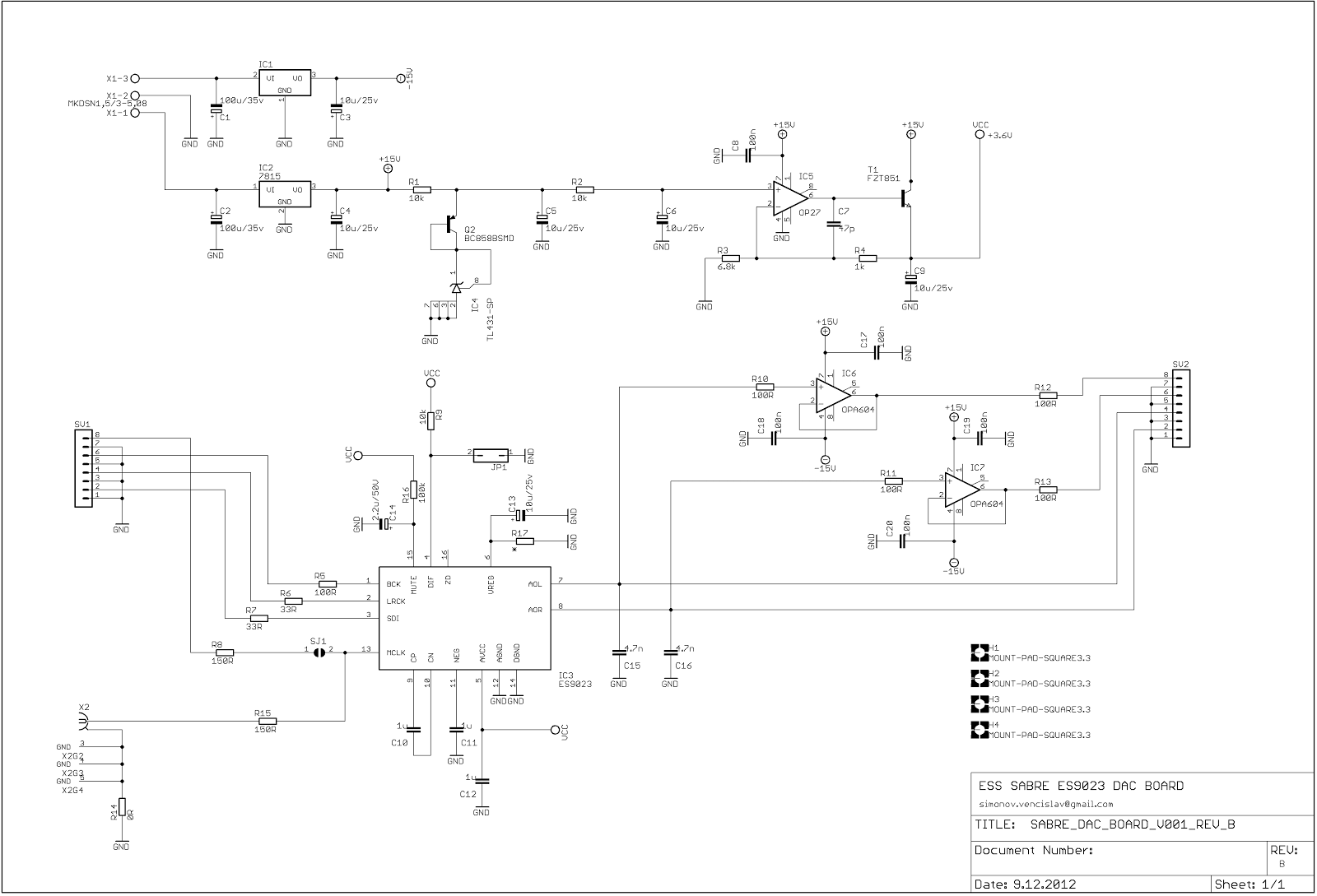
So this is what the schematic looks like:
You might note that the DAC is powered by 3.6V (and not the standard 3.3V). This is due to the output swing hitting the supply rails. The chip has an internal charge pump that generates the negative rail so that the output signal is centered around the 0V (no coupling capacitor required). The manufacturer had increased the supply voltage to 3.6V to prevent the output stage from clipping.
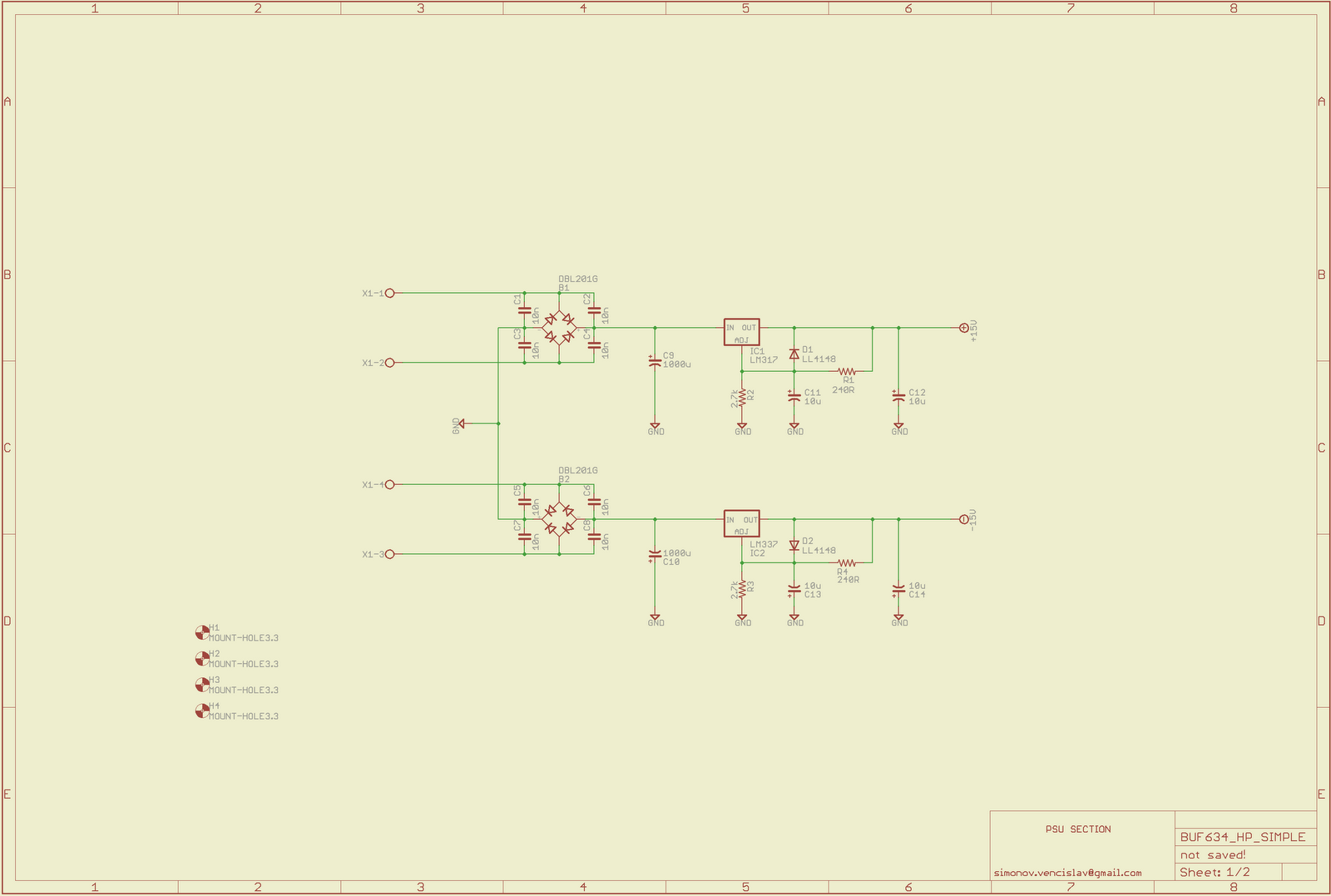
Few words about the power supply circuit. The output buffer formed bu IC6 and IC7 is powered by a simple voltage regulators 7815 and 7915. Nothing interesting here. The DAC chip is powered by a low noise low dropout voltage regulator with a series pass element. Q2 and IC4 form a voltage reference. Its output is filtered by a low-pass filter formed by R2 and C6 and fed to the non-inverting pin of a low-noise opamp IC5. The output voltage is set by the two feedback resistors R3 and R4. C7 is placed across the opamp to improve stability.
The overall noise performance of this regulator is outstanding. The opamp’s noise is critical. For lower cost version you can use NE5534 but some additional compensation is required. Don’t forget to include a 33-68pF capacitor between pins 5 and 8.
I have included an input for an external clock source. This is implemented with one SMB connector. The solder joint SJ1 serves as a switch point. If you are using the external clock SJ1 must be desoldered.
The jumper JP1 is there to set the input format. It can be either left justified or Philips – I2S. The JP1 settings a re the following:
JP1 – CLOSED – I2S
JP1 – OPEN – LEFT JUSTIFIED
The output buffer stage is formed by two unity gain opamps. Those are subject to a personal taste of course. I have made the PCB with sockets to make it easier to switch the opamps.
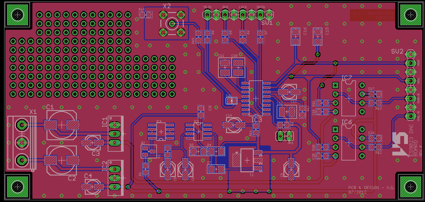
This is how the pcb looks like:
The PCB has a small prototyping area just in case. Many modifications might be needed so its always a good thing to have some place for additional components.
I’m including a complete project manufacturing files available for download HERE
EAGLE BRD file – HERE
Update 09.12.2012 – I have made some changes to design. Revision B is now available for download.
Update 22.03.2013 – Added EAGLE *.brd files for downloading
THIS PROJECT IS AVAILABLE FOR PERSONAL USE ONLY. COMMERCIAL USE OR MANUFACTURING PCB’S FOR SALE IS NOT ALLOWED.
THANK YOU FOR READING THIS ARTICLE