AUDIO WORKSHOP

DIY audio blog for projects, schematics, PCB's, designs, electronics, mods

AUDIO_WORKSHOP

PCM1704, AD1862 DAC, NOS, DIY schematic

Non oversampling DACs are by many people (includung me) regarded as better sounding than
conventional oversampling systems. The easiest way to enjoy that kind of sound is to build a DAC with the “outdated” TDA1543/TDA1541 DAC ICs or modify an old Philips/Marantz CD player.

But why not building a nonos DAC with higher quality converters like PCM1704, PCM1702 or AD1862? Well, you need to convert serial DATA to parallel DATA which requires some glue logic. Further glue logic is needed to align 16bit DATA with the 20bit or 24bit inputs of these DAC ICs.
While there are many well documented TDA based nonos projects available on the www, almost nothing can be found about building a nonos DAC with more recent Burr Brown / Analog Device ICs. That’s why I’ll try to give some advice and share some of my experience in building such a DAC. If there wouldn’t be this glue logic issue, I guess more DIYer would build nonos DACs with Burr Brown chips.

Creating a DIY non oversampling DAC with PCM1704 >>>[ LINK ]<<<

BUF634 Headphone Amplifier, Driver. PCB Project.

Here is a project describing a very high quality headphone amplifier built around the TI’s buffer IC – BUF634. The project features a complete design including PSU section, input section, volume control and output connector.
The whole design is completely DC coupled form input to output. The BUF634 IC was used to boost the output current of the op-amp forming the input stage of the amplifier.

In order to keep the DC offset at the output low enough it is recommended to use precision op-amps like OPA132. FET input is preferable. This gives you high input impedance and low gain error. Of course for really low cost application one can you the traditional NE5534. However you may need to set a small compensation capacitor across pin 5 and pin 8 of 5534. A value of about 10pF would be enough. The other way is to have the stage gain set at higher value. Resistors R9/R8 and R14/R13 set the gain of the stage. With the default values the gain is set at about 15dB or G=5.7

The schematic for this project looks like this:

BUF634 AMPLIFIER SCHEMATIC

Few words about the schematic. The input potentiometer is ALPS RK27 series. Dual pot logarithmic. Value 20K.

The input signal is passed through a low-pass RC filter formed by R5/C15 and R10/C22. Omitting this filter will cause a small overshoot when testing with square wave. Bare in mined that BUF634 is a wide bandwidth IC (so are the input op-amps). Some form of high frequency suppression is good to have as we are only dealing with audio frequencies here.

The output connector is Neutrik NMJ6 PCB mount series.

The PSU:

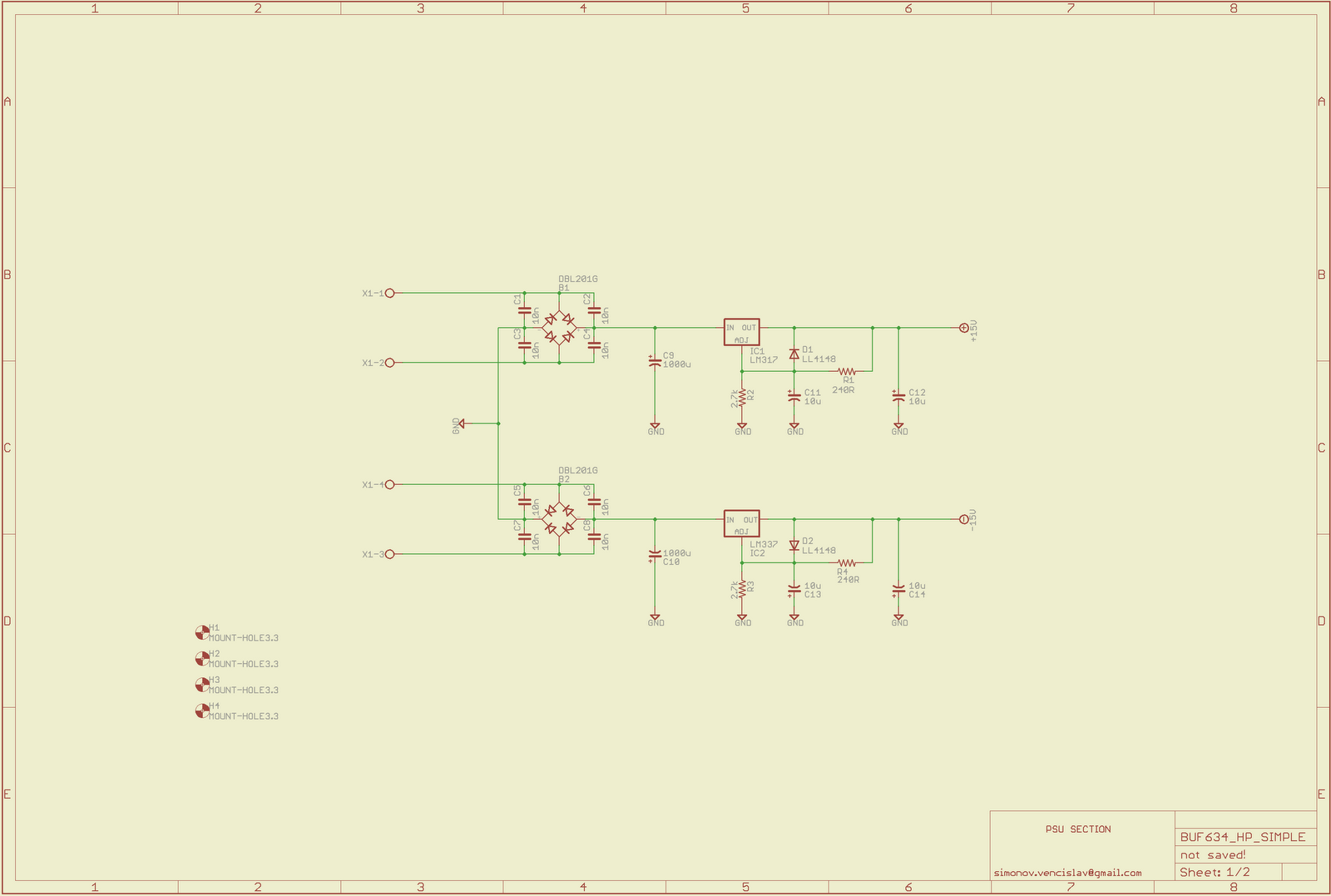
BUF_634_HEADPHONE_AMPLIFIER_POWER_SUPPLY_SCHEMATIC
BUF634 HEADPHONE AMPLIFIER POWER SUPPLY

The power supply is a bit nontraditional. It uses two bridge rectifiers to form the two power supply rails and the GND. This means you will need a transformer with TWO SEPARATE secondary winding. 30VA transformer providing about 2x17VAC is sufficient to power this amplifier. The decoupling capacitors around the optional. Those are suppose to reduce the noise coming from the diodes. I have never actually been able to hear any audible difference between “bypassed” and “non bypassed” bridge rectifiers so I leave that to your own personal judgement. Mounted or not one thig is for sure – they do no harm. The rest of the PSU is pretty straightforward. It is regulated power supply using the traditional LM317/LM337 regulators.

From the power supply each rail is then delivered to the op-amps trough individual LC filtering.

The PCB:

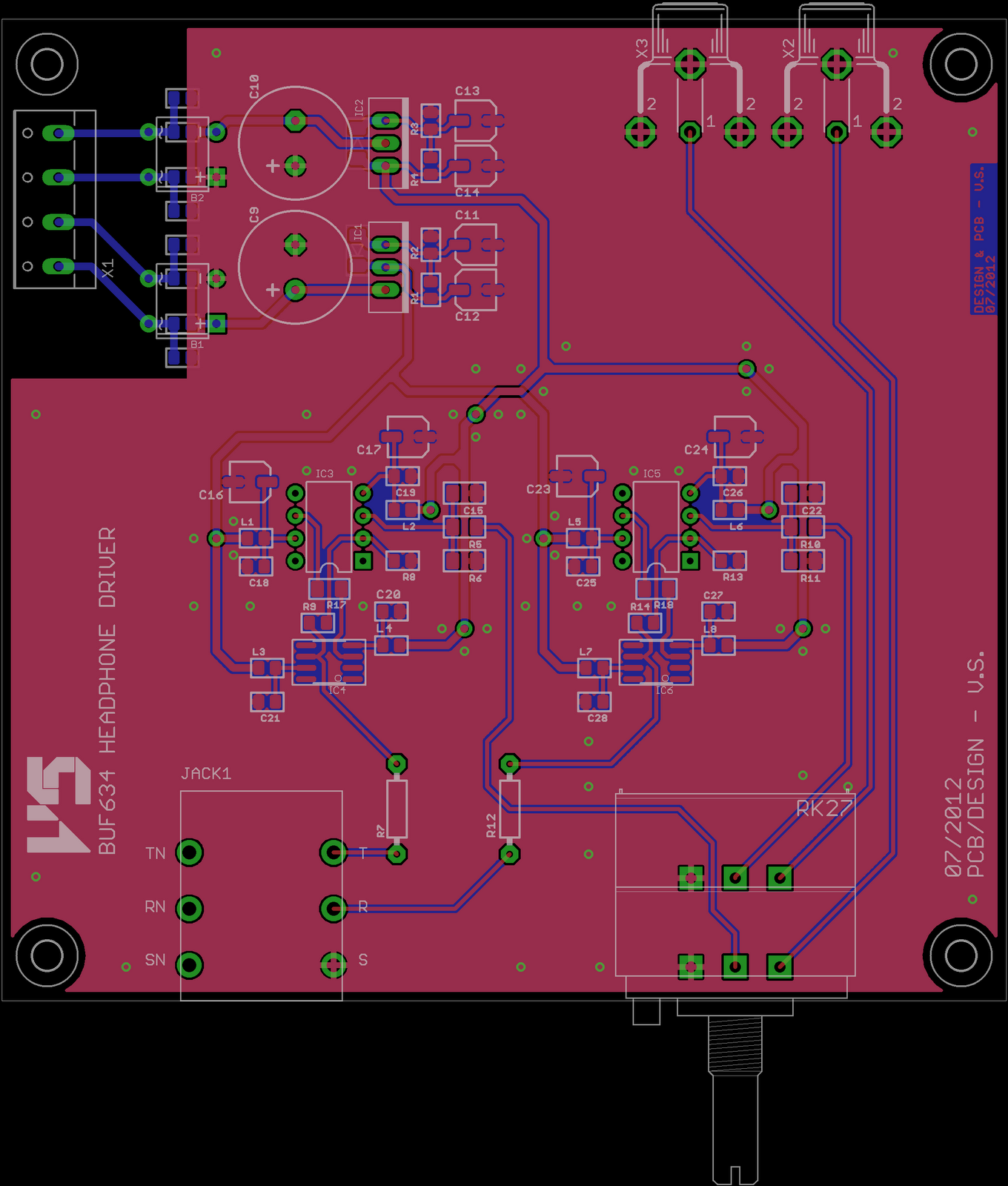
buf634_amplifier_headphone_pcb
BUF634 HEADPHONE AMPLIFIER PCB

The PCB is two sided with large GND copper pour for improved noise and parasitic interference shielding. The two input op-amps are in DIP package to allow for further experimentation. Those are in many of the cases, a subject to personal taste. However I’m giving a small list of op-amps that in my opinion are suitable for this project:
LT1022, LT1468, LT1028, OPA602, OPA604, OPA227

Complete parts list:
Partlist exported from C:/Program Files (x86)/EAGLE-5.11.0/projects/BUF634/BUF634_HP_SIMPLE.sch at 25.7.2012 г. 14:21:49 ч.

Part  Value         Device         Package        Description
B1    DBL201G       DBL201G        DB      Single Phase 1.0 AMP Glass Passivated Bridge Rectifier
B2    DBL201G       DBL201G        DB      Single Phase 1.0 AMP Glass Passivated Bridge Rectifier
C1    10n           C_0805         C0805          NON-POLARIZED CAP
C2    10n           C_0805         C0805          NON-POLARIZED CAP
C3    10n           C_0805         C0805          NON-POLARIZED CAP
C4    10n           C_0805         C0805          NON-POLARIZED CAP
C5    10n           C_0805         C0805          NON-POLARIZED CAP
C6    10n           C_0805         C0805          NON-POLARIZED CAP
C7    10n           C_0805         C0805          NON-POLARIZED CAP
C8    10n           C_0805         C0805          NON-POLARIZED CAP
C9    1000u         CP_E-050X125   CE-050X125     POLARIZED CAP
C10   1000u         CP_E-050X125   CE-050X125     POLARIZED CAP
C11   10u           CP_SV-B        CSV-B          POLARIZED CAP
C12   10u           CP_SV-B        CSV-B          POLARIZED CAP
C13   10u           CP_SV-B        CSV-B          POLARIZED CAP
C14   10u           CP_SV-B        CSV-B          POLARIZED CAP
C15   150p          C_1206         C1206          NON-POLARIZED CAP
C16   10u           CP_SV-B        CSV-B          POLARIZED CAP
C17   10u           CP_SV-B        CSV-B          POLARIZED CAP
C18   10n           C_0805         C0805          NON-POLARIZED CAP
C19   10n           C_0805         C0805          NON-POLARIZED CAP
C20   10n           C_0805         C0805          NON-POLARIZED CAP
C21   10n           C_0805         C0805          NON-POLARIZED CAP
C22   150p          C_1206         C1206          NON-POLARIZED CAP
C23   10u           CP_SV-B        CSV-B          POLARIZED CAP
C24   10u           CP_SV-B        CSV-B          POLARIZED CAP
C25   10n           C_0805         C0805          NON-POLARIZED CAP
C26   10n           C_0805         C0805          NON-POLARIZED CAP
C27   10n           C_0805         C0805          NON-POLARIZED CAP
C28   10n           C_0805         C0805          NON-POLARIZED CAP
D1    LL4148        DIODE-MINIMELF MINIMELF       DIODE
D2    LL4148        DIODE-MINIMELF MINIMELF       DIODE
IC1   LM317         LM317TS        317TS          VOLTAGE REGULATOR
IC2   LM337         LM337TS        337TS          VOLTAGE REGULATOR
IC3   OPA132        OPA134P        DIL08          Operational Amplifiers
IC4   BUF634U       BUF634U        SO08           250mA High-Speed Buffer
IC5   OPA132        OPA134P        DIL08          Operational Amplifiers
IC6   BUF634U       BUF634U        SO08           250mA High-Speed Buffer
L1    1.0uH/92mA/6.90Ω          L_0805         L0805          INDUCTOR
L2    1.0uH/92mA/6.90Ω          L_0805         L0805          INDUCTOR
L3    1.0uH/92mA/6.90Ω          L_0805         L0805          INDUCTOR
L4    1.0uH/92mA/6.90Ω          L_0805         L0805          INDUCTOR
L5    1.0uH/92mA/6.90Ω          L_0805         L0805          INDUCTOR
L6    1.0uH/92mA/6.90Ω          L_0805         L0805          INDUCTOR
L7    1.0uH/92mA/6.90Ω          L_0805         L0805          INDUCTOR
L8    1.0uH/92mA/6.90Ω          L_0805         L0805          INDUCTOR
POT1  RK27-DUAL-20K RK27-DUAL      RK27-DUAL-UNIT
R1    240R          R_0805         R0805          RESISTOR
R2    2.7k          R_0805         R0805          RESISTOR
R3    2.7k          R_0805         R0805          RESISTOR
R4    240R          R_0805         R0805          RESISTOR
R5    1k            R_1206         R1206          RESISTOR
R6    22k           R_1206         R1206          RESISTOR
R7    10R           R_X0207/10C    0207/10C       RESISTOR
R8    1k            R_0805         R0805          RESISTOR
R9    4.7K          R_0805         R0805          RESISTOR
R10   1k            R_1206         R1206          RESISTOR
R11   22k           R_1206         R1206          RESISTOR
R12   10R           R_X0207/10C    0207/10C       RESISTOR
R13   1k            R_0805         R0805          RESISTOR
R14   4.7K          R_0805         R0805          RESISTOR
R17   10R           R_1206W        R1206W         RESISTOR
R18   10R           R_1206W        R1206W         RESISTOR
Complete manufacturing files are available for download HERE

THIS PROJECT IS AVAILABLE FOR DIY AND PERSONAL USE ONLY. COMMERCIAL USE IS NOT ALLOWED WITHOUT AUTHOR’S EXCLUSIVE PERMISSION!

THANK YOU FOR READING!!!

IL715 Digital Isolator PCB Design

This project is based on the IL715 digital isolator chip, manufactured by NVE Corporation. This is a simple isolator schematic and a PCB.
Here is the technical datasheet for this chip:

[LINK]

The IC is pretty easy to use. They made the pinout as suitable as it can be. For this project I decided to make a sort of an adapter PCB which can be mounted on suitable female headers to the main PCB. I also decided to put a local voltage regulation just to be on the safe side. Local voltage regulation is proven to a good practice. I’m not quite sure if it serves a good purpose in this particular project but it does no harm either 😉

Of course from the datasheet you can see that there are several variants to this chip depending on the needs. The PCB itself does not change so it’s suitable for all the types. For example when doing a local reclocking near the DAC ship and driving a master clock directly to the DAC’s form external master clock source, you will need to send this clock back to the digital part of the system. This one will feed the digital filter and the servo processor(and of course all the other IC’s that need a clock supply). In this case you can use IL717 IC.

The schematic itself is pretty straightforward as the application is a no challenge to any designer. This is what it looks like:

IL715 Digital Isolator PCB, Schematic design
IL715, IL716, IL717 DIGITAL ISOLATOR SCHEMATIC

And this is the PCB:

IL715 Digital Isolator PCB
IL715, IL716, IL717 DIGITAL ISOLATOR PCB

The complete manufacturing files are available for download HERE

This project is provided to the DIY community for free. Commercial use is not allowed!

!!!THANK YOU FOR READING THIS ARTICLE!!!
_

AutoCAD to EAGLE PCB Drawing Import

Drawing a PCB by exact dimensions using EAGLE PCB isn’t quite the easy thing. An easier approach would be to draw it in AutoCAD and then import.

Importing is quite easy. This is how it goes. This is my simple pcb 😀

Now what you need is to save the drawing to DXF format by going to Save As and chose AutoCAD 2004 DXF form the Files of type drop down menu. Name your file and save it.

Now you need to convert this file to something that EAGLE would understand – a script. For this to work I use a simple DXF so SCR converter by http://www.micromagicsystems.com/

Here is the app:

DXF TO SCR CONVERTER

Load the file and hit convert. You need to provide destination for both input and output file.

Now you go to EAGLE PCB and select File -> Script. Find the SCR file and open it. Now you should see the exact same PCB form the AutoCAD drawing.

However you will need to place holes and drills. Those you see now are drawn on the Dimensions layer AND WILL NOT FORM ANY ACTUAL DRILLS. Here is a trick that helps me dealing with this.

It is wise to put some sort of a mark for the center of the holes when drawing the PCB in AutoCAD. A small cross would do just fine. After  importing the drawing to EAGLE those crosses will be used as a markers to show the exact place of the holes and drills. This is how I do it:

After the import you need to zoom in to the center. Turn your grid on (I use dots) and carefully align the center of the hole and the marker. Take note that after the import the grid is set to Finest(which is 1 mil) You might need to use the Change command to make the lines 0 mils in width. It’s easier to see the grid this way. Now use the move command to get the hole or drill. The holes are usually placed on the schematic so they have names like H1, H2 .. etc. To grab the hole just type its name in the command line.

 You might need to zoom even further O.O  :

It is a tricky job but with some practice you will get used to it 🙂 When you are finished aligning the holes you can delete the markers. Now you change your grid back to normal.

THANK YOU FOR READING THIS ARTICLE

ESS ES9023 SABRE DAC BOARD

This project is about the ESS Sabre ES2093 DAC chip. This one is the least expensive DAC chip from the whole line up of DAC’s manufactured by ESS Technology. What i wanted to do here is to make something like an evaluation board which can be almost universal.

ESS Technology might not be quite a famous among audiophiles or electronics fans. They have this kinda odd marketing policy that puts them on the edge of OEM and retail markets. However thy are manufacturing some very high specs chips (DAC’s and ADC’s) and supply them to many manufacturers of high quality AV components like OPPO and many others.

The famous Buffalo DAC is built around an ESS 32-bit DAC. More info on this one can be found here:
http://www.twistedpearaudio.com/digital/buffalo.aspx

Of course with this project I’m not aiming on beating a complete high-end DAC’s like the Buffalo. What I want is to have this board as an upgrade to any low-end delta-sigma DAC. Besides the fact that it is a low-cost chip does not mean that it’s not worth a try. I believe that a proper designed board and a good power supply can make a low-cost DAC like the ES9023 sound very good. The history knows some good examples of CD players using low-cost DAC’s but sounding very good indeed.

More info about the ES9023 DAC chip can be found here:

http://www.esstech.com/PDF/ES9023%20PB%20Rev%200.2aPB%20110117.pdf

Unfortunately this is just a product brief but it gives some basic information. Due to the ESS Technology policy I can post the complete technical datasheet. If you want to have it you would need to contact some of the local ESS Technology distributors.

As you can see this little DAC offers a complete solution. It includes digital filtering, DAC, and output stage. However I’m including a buffer option on the PCB as I don’t really know the driving capabilities of the DAC alone. Some fancy cables actually have huge parasitic capacitance and can make the life hard for the little DAC.

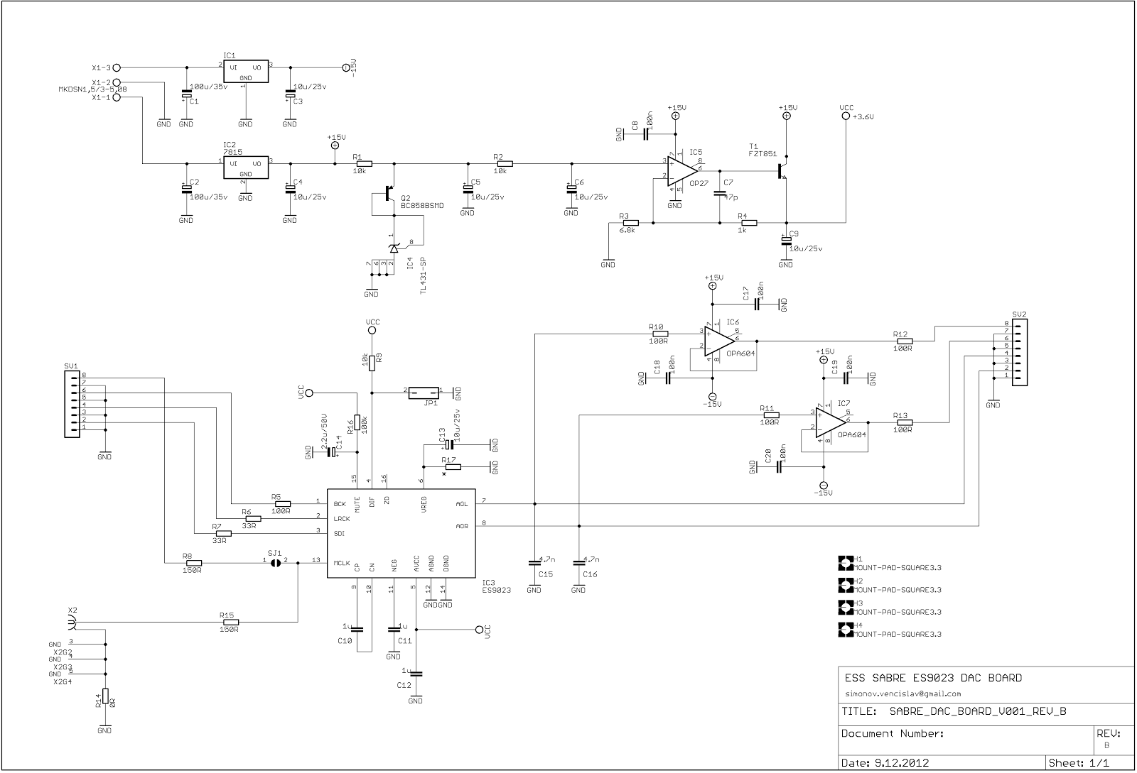
So this is what the schematic looks like:

ES9023_DAC_SCHEMATIC_AUDIO

You might note that the DAC is powered by 3.6V (and not the standard 3.3V). This is due to the output swing hitting the supply rails. The chip has an internal charge pump that generates the negative rail so that the output signal is centered around the 0V (no coupling capacitor required). The manufacturer had increased the supply voltage to 3.6V to prevent the output stage from clipping.

Few words about the power supply circuit. The output buffer formed bu IC6 and IC7 is powered by a simple voltage regulators 7815 and 7915. Nothing interesting here. The DAC chip is powered by a low noise low dropout voltage regulator with a series pass element. Q2 and IC4 form a voltage reference. Its output is filtered by a low-pass filter formed by R2 and C6 and fed to the non-inverting pin of a low-noise opamp IC5. The output voltage is set by the two feedback resistors R3 and R4. C7 is placed across the opamp to improve stability.

The overall noise performance of this regulator is outstanding. The opamp’s noise is critical. For lower cost version you can use NE5534 but some additional compensation is required. Don’t forget to include a 33-68pF capacitor between pins 5 and 8.

I have included an input for an external clock source. This is implemented with one SMB connector. The solder joint SJ1 serves as a switch point. If you are using the external clock SJ1 must be desoldered.

The jumper JP1 is there to set the input format. It can be either left justified or Philips – I2S. The JP1 settings a re the following:

JP1 – CLOSED – I2S
JP1 – OPEN – LEFT JUSTIFIED

The output buffer stage is formed by two unity gain opamps. Those are subject to a personal taste of course. I have made the PCB with sockets to make it easier to switch the opamps.

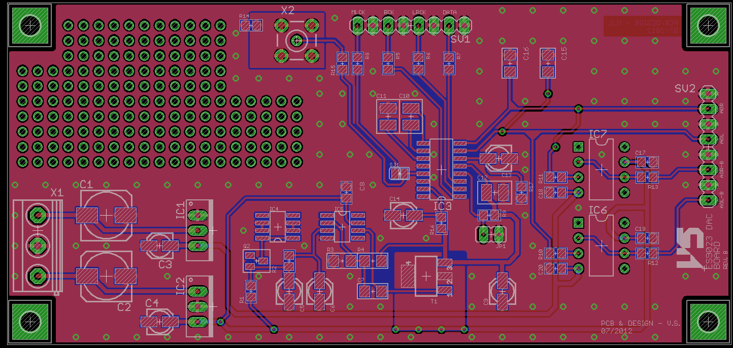
This is how the pcb looks like:

ES9023_DAC_PCB_AUDIO

The PCB has a small prototyping area just in case. Many modifications might be needed so its always a good thing to have some place for additional components.

I’m including a complete project manufacturing files available for download HERE

EAGLE BRD file – HERE

Update 09.12.2012 – I have made some changes to design. Revision B is now available for download.

Update 22.03.2013 – Added EAGLE *.brd files for downloading

THIS PROJECT IS AVAILABLE FOR PERSONAL USE ONLY. COMMERCIAL USE OR MANUFACTURING PCB’S FOR SALE IS NOT ALLOWED.

THANK YOU FOR READING THIS ARTICLE

Page 8 of 11

Powered by WordPress & Theme by Anders Norén

AUDIO WORKSHOP